

VACCO’s Multi-Fab group offers Micro Laser Cutting Services for precision laser cutting, micro welding, marking or other machining. VACCO’s laser capabilities are complementary to the markets served because of the demands placed for complete fabricated components on a turnkey basis.
VACCO’s Micro Laser Services of the thin metal and polyamide product market further benefit many companies that rely on VACCO as their quality component supplier. The added value of Micro Laser Services allows for quicker deliveries, and aids in producing products not currently available through the photo etching process. Many OEM customers have taken action to reduce their vendor list and VACCO is helping these companies by proactively being a complete “one stop-shop.”
Reducing lead-times, and costs with the flexibility of getting a one stop component service capability is something industry is always asking for and VACCO’s Micro Laser Services can deliver. VACCO also provides assistance on material selection. Depending on a client’s requirements certain materials may be better suited for the environment.
VACCO produces components for many industries including: Avionics, Medical, Electronics and Research applications. The range of process capabilities VACCO allows design engineers the benefits of lower costs, faster delivery and part design flexibility.
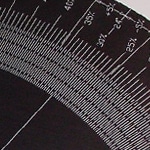
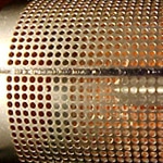
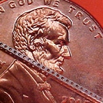
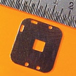
Positional accuracy of ± 1 micrometer and repeatability of ± 0.5 micrometer is common place with Micro Laser Services. Welding has deep penetration and spot welding can be as small as 0.005″. In some cases, “Hole-to-Material” drilling can be as great as a 10:1 ratio.
Problems Addressed Though VACCO Micro Laser Services
Many precision components require features, tolerances, or geometries that traditional machining or photo etching cannot achieve. Micro laser processing helps solve challenges such as:
- Difficulty producing extremely small holes, slots, or apertures with consistent accuracy.
- Need for clean edges without burrs or thermal distortion.
- Limitations in joining thin metals or polyamide materials using conventional welding.
- Long lead times when multiple vendors are required for cutting, welding, and marking.
- Inability to fabricate certain part designs using photo etching alone.
Micro laser services provide a flexible solution for producing intricate features while supporting fast turnaround and consolidated manufacturing.
Design Considerations
Micro laser processing offers significant flexibility, but certain design factors help ensure optimal results. Key considerations include:
- Minimum feature size and spacing for apertures, slots, and micro holes.
- Material type and thickness, especially for thin metals and polyamides.
- Required edge quality for optical, electronic, or medical applications.
- Tolerance requirements for positional accuracy and repeatability.
- Whether the part requires cutting, welding, marking, or a combination of processes.
Early collaboration with engineering helps ensure designs take full advantage of the precision and versatility of laser processing.
Micro Laser Cutting Services Frequently Asked Questions
What Types of Features Can Be Produced with Micro Laser Cutting Services?
Micro laser cutting services can help create fine holes, slots, apertures, welds, and markings with high accuracy, including features as small as 0.005″.
Which Materials Are Compatible with Micro Laser Processing?
Thin metals and polyamide materials are commonly processed, with material selection guided by application requirements.
How Accurate Is the Process?
Positional accuracy of ±1 micrometer and repeatability of ±0.5 micrometer is typical for micro laser operations.
Micro Laser Capabilities
Primary Services
- Cutting
- Marking
- Welding
Material List
Please visit Photo Chemical Etching Process for more information.
Material Thickness
.001″ to .075″ (.25mm to 1.9mm)
Maximum Panel Size
Material panels as large as 16” x 16”
Minimum Dimensional Tolerance
Capable of +/-1 micrometer and repeatability of +/-0.5 micrometer.
Positioning Accuracy
Capable of +/-1 micrometer and repeatability of +/-0.5 micrometer.
Through Holes Size
10:1 Hole-to-Material thickness ratio capability
Aperture Sizes
Holes as small as .002″
Pitch
On-centers as small as .004″
Aspect Ratios/level
10:1
Applications
- Avionics
- Embossing Micro Parts
- Filtration/Microfiltration
- Laboratory and Test Masking
- Micro-channels
- Micro-circuitry
- Micro-embossing Tools
- Micro-reactors and Lab-on-chip
- Micro-replication of Silicon Masters
- Precision filters, mesh, and sieves
Industries Served
- Avionic/Space Electronics
- Mechanical/
Manufacturing
- Medical
- Research Applications
- Scientific Controls
Certifications
- Clean Room Accredited to FED-STD-209 Class 10,000 Standards
- PRI / NADCAP Certified
- AS9100
Software Used
- AutoCAD
- Autodesk Inventor
Acceptable File Formats
- DWG
- DXF
- IGES
- JPEG
- STP