


What is Electroforming?
Electroforming is an additive process in which nickel is deposited in a platting process around a substrate created from a photolithographic pattern. This forms a self-supporting structure with consistent surface finishes and dimensional stability.
Electroforming allows parts to be created with tight tolerances (up to +/- 2 µm), superior edge finishes, and ultra-fine features (as small as 15 µm). The average parts produced range from .001 inch (25 µm) to .006 inch (15 µm) thick. If necessary, they can be made as thin as .0003 inch (8 µm) to as thick as .006 inch (150 µm). These parts can be produced in material panels as large as 20 x 20 inches.
The nickel composition used in electroforming can be specified to meet certain requirements, including the degree of hardness, finish and brightness, and malleability.
Parts, including screens that need structural support in ultra-thin layers, can be produced using multi-level designs and support grids.
The advantages of Electroformed Parts and Screens
- Parts can have mirror-like finish on front and back
- No visible grain direction
- Tab free parts
- Tolerances generally +/- .0003” (8 µm) but vary slightly by application
- Low Cost Tooling
- Quick turnaround time, generally less than 2 weeks
Typical Products
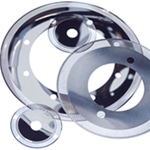
- Metal Encoders Wheels
- Electroformed Screens
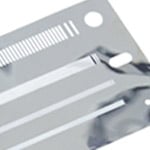
- Lead Frames
- Printer Components
- Shadow / Deposition Masks
- Micro Filters
- Micro Valves
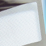
- Wire Mesh (as small as 1,000 mesh)
- Molds
- Sieves
Markets / Industries
- Filtration
- Medical
- Electronics
- Masking
- Avionics
- Aerospace
- Life Sciences
- Electronics
- Textile
- Printer
Problems Addressed Through VACCO Electroforming
Electroforming is often selected when traditional manufacturing methods cannot achieve the precision or surface quality required. Common challenges include:
- Difficulty producing ultra fine features smaller than machining or stamping can support.
- Need for smooth, uniform surfaces without secondary finishing.
- Limitations in forming thin wall structures that remain self supporting.
- High tooling costs associated with conventional fabrication.
- Inconsistent thickness or dimensional variation across complex geometries.
Electroforming helps overcome these issues by creating highly accurate, repeatable metal components with excellent surface finishes.
Design Considerations
Electroforming offers significant flexibility, but certain design factors help ensure optimal results. Key considerations include:
- Feature size and spacing, especially for micro patterns or fine meshes.
- Required thickness range and uniformity across the part.
- Need for multi level structures or integrated support grids.
- Surface finish requirements for optical, filtration, or electronic applications.
- Panel size constraints for high volume production.
Early collaboration during the design phase helps ensure that parts take full advantage of the process’s precision and repeatability.
Electroforming Frequently Asked Questions
What Types of Features Can Electroforming Produce?
Electroforming can create ultra fine features, smooth surfaces, and thin wall structures that are difficult to achieve with subtractive methods.
How Thin or Thick Can Electroformed Parts Be?
Typical thicknesses range from .001 inch to .006 inch, with options as thin as .0003 inch depending on application needs.
What Materials Are Used in Electroforming?
Nickel is the primary material, with compositions tailored for hardness, brightness, finish, and malleability.
Is Electroforming Suitable for High Volume Production?
Yes. The process supports rapid replication of photolithographic patterns, making it suitable for both prototyping and large scale manufacturing.